- 您现在的位置:买卖IC网 > Sheet目录1214 > EVAL-ADE7880EBZ (Analog Devices Inc)BOARD EVAL FOR ADE7880
�� �
�
�Data� Sheet�
�POWER� QUALITY� MEASUREMENTS�
�Zero-Crossing� Detection�
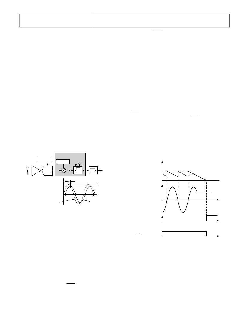
�The� ADE7880� has� a� zero-crossing� (ZX)� detection� circuit� on� the�
�phase� current� and� voltage� channels.� The� neutral� current� data�
�path� does� not� contain� a� zero-crossing� detection� circuit.� Zero-�
�crossing� events� are� used� as� a� time� base� for� various� power� quality�
�measurements� and� in� the� calibration� process.�
�The� output� of� LPF1� is� used� to� generate� zero� crossing� events.�
�The� low-pass� filter� is� intended� to� eliminate� all� harmonics� of�
�50� Hz� and� 60� Hz� systems,� and� to� help� identify� the� zero-crossing�
�events� on� the� fundamental� components� of� both� current� and�
�voltage� channels.�
�The� digital� filter� has� a� pole� at� 80� Hz� and� is� clocked� at� 256� kHz.�
�As� a� result,� there� is� a� phase� lag� between� the� analog� input� signal�
�(one� of� IA,� IB,� IC,� VA,� VB,� and� VC)� and� the� output� of� LPF1.�
�The� error� in� ZX� detection� is� 0.0703°� for� 50� Hz� systems� (0.0843°�
�for� 60� Hz� systems).� The� phase� lag� response� of� LPF1� results� in� a�
�time� delay� of� approximately� 31.4°� or� 1.74� ms� (at� 50� Hz)� between�
�its� input� and� output.� The� overall� delay� between� the� zero� crossing�
�on� the� analog� inputs� and� ZX� detection� obtained� after� LPF1� is�
�about� 39.6°� or� 2.2� ms� (at� 50� Hz).� The� ADC� and� HPF� introduce�
�the� additional� delay.� The� LPF1� cannot� be� disabled� to� assure� a�
�good� resolution� of� the� ZX� detection.� Figure� 50� shows� how� the�
�zero-crossing� signal� is� detected.�
�ADE7880�
�cleared� and� the� IRQ1� pin� is� set� to� high� by� writing� to� the� STATUS1�
�register� with� the� status� bit� set� to� 1.�
�Zero-Crossing� Timeout�
�Every� zero-crossing� detection� circuit� has� an� associated� timeout�
�register.� This� register� is� loaded� with� the� value� written� into� the�
�16-bit� ZXTOUT� register� and� is� decremented� (1� LSB)� every�
�62.5� μs� (16� kHz� clock).� The� register� is� reset� to� the� ZXTOUT�
�value� every� time� a� zero� crossing� is� detected.� The� default� value� of�
�this� register� is� 0xFFFF.� If� the� timeout� register� decrements� to� 0�
�before� a� zero� crossing� is� detected,� one� of� Bits[8:3]� of� the� STATUS1�
�register� is� set� to� 1.� Bit� 3� (ZXTOVA),� Bit� 4� (ZXTOVB),� and� Bit� 5�
�(ZXTOVC)� in� the� STATUS1� register� refer� to� Phase� A,� Phase� B,�
�and� Phase� C� of� the� voltage� channel;� Bit� 6� (ZXTOIA),� Bit� 7�
�(ZXTOIB),� and� Bit� 8� (ZXTOIC)� in� the� STATUS1� register� refer�
�to� Phase� A,� Phase� B,� and� Phase� C� of� the� current� channel.�
�If� a� ZXTOIx� or� ZXTOVx� bit� is� set� in� the� MASK1� register,� the�
�IRQ1� interrupt� pin� is� driven� low� when� the� corresponding� status� bit�
�is� set� to� 1.� The� status� bit� is� cleared� and� the� IRQ1� pin� is� returned� to�
�high� by� writing� to� the� STATUS1� register� with� the� status� bit� set� to� 1.�
�The� resolution� of� the� ZXOUT� register� is� 62.5� μs� (16� kHz� clock)�
�per� LSB.� Thus,� the� maximum� timeout� period� for� an� interrupt� is�
�4.096� sec:� 2� 16� /16� kHz.�
��detection� when� the� voltage� or� the� current� signal� stays� at� a� fixed�
�IA,� IB,� IC,�
�OR�
�VA,� VB,� VC�
�PGA�
�REFERENCE�
�ADC�
�DSP�
�HPFEN� BIT�
�GAIN[23:0]� CONFIG3[0]�
�HPF�
�LPF1�
�ZX�
�DETECTION�
�dc� level� for� more� than� 62.5� μs� ×� ZXTOUT� μs.�
�16-BIT� INTERNAL�
�REGISTER� VALUE�
�ZXTOUT�
�1�
�0.855�
�39.6°� OR� 2.2ms� @� 50Hz�
�0V�
�IA,� IB,� IC,� IN�
�OR�
�VA,� VB,� VC�
�ZX�
�ZX�
�ZX�
�ZX�
�LPF1� OUTPUT�
�VOLTAGE�
�OR�
�CURRENT�
�SIGNAL�
�0V�
�Figure� 50.� Zero-Crossing� Detection� on� Voltage� and� Current� Channels�
�To� provide� further� protection� from� noise,� input� signals� to� the�
�voltage� channel� with� amplitude� lower� than� 10%� of� full� scale� do�
�not� generate� zero-crossing� events� at� all.� The� Current� Channel� ZX�
�detection� circuit� is� active� for� all� input� signals� independent� of� their�
�amplitudes.�
�The� ADE7880� contains� six� zero-crossing� detection� circuits,� one�
�for� each� phase� voltage� and� current� channel.� Each� circuit� drives�
�one� flag� in� the� STATUS1� register.� If� a� circuit� placed� in� the� Phase�
�A� voltage� channel� detects� one� zero-crossing� event,� Bit� 9� (ZXVA)�
�in� the� STATUS1� register� is� set� to� 1.�
�Similarly,� the� Phase� B� voltage� circuit� drives� Bit� 10� (ZXVB),� the�
�Phase� C� voltage� circuit� drives� Bit� 11� (ZXVC),� and� circuits� placed�
�in� the� current� channel� drive� Bit� 12� (ZXIA),� Bit� 13� (ZXIB),� and�
�Bit� 14� (ZXIC)� in� the� STATUS1� register.� If� a� ZX� detection� bit� is�
�set� in� the� MASK1� register,� the� IRQ1� interrupt� pin� is� driven� low�
�ZXZOxy� FLAG� IN�
�STATUS1[31:0],� x� =� V,� A�
�y� =� A,� B,� C�
�IRQ1� INTERRUPT� PIN�
�Figure� 51.� Zero-Crossing� Timeout� Detection�
�Phase� Sequence� Detection�
�The� ADE7880� has� on-chip� phase� sequence� error� detection�
�circuits.� This� detection� works� on� phase� voltages� and� considers�
�only� the� zero� crossings� determined� by� their� negative-to-positive�
�transitions.� The� regular� succession� of� these� zero-crossing� events� is�
�Phase� A� followed� by� Phase� B� followed� by� Phase� C� (see� Figure� 53).�
�If� the� sequence� of� zero-crossing� events� is,� instead,� Phase� A� followed�
�by� Phase� C� followed� by� Phase� B,� then� Bit� 19� (SEQERR)� in� the�
�STATUS1� register� is� set.�
�and� the� corresponding� status� flag� is� set� to� 1.� The� status� bit� is�
�Rev.� A� |� Page� 31� of� 104�
�发布紧急采购,3分钟左右您将得到回复。
相关PDF资料
EVAL-ADE7953EBZ
BOARD EVAL FOR ADE7953
EVAL-ADF4002EBZ1
BOARD EVAL FOR ADF4002
EVAL-ADG788EBZ
BOARD EVALUATION FOR ADG788
EVAL-ADM1021AEB
BOARD EVAL FOR ADM1021
EVAL-ADM1023EB
BOARD EVAL FOR ADM1023
EVAL-ADM1031EB
BOARD EVAL FOR ADM1031
EVAL-ADM1062TQEBZ
BOARD EVALUATION FOR ADM1062TQ
EVAL-ADM1075CEBZ
BOARD EVAL FOR ADM1075
相关代理商/技术参数
EVAL-ADE7880EBZ
制造商:Analog Devices 功能描述:ADE7880, ENERGY METER, 3 PH, SPI, I2C, E
EVAL-ADE7913EBZ
制造商:AD 制造商全称:Analog Devices 功能描述:3-Channel, Isolated, Sigma-Delta ADC with SPI
EVAL-ADE7953EBZ
功能描述:BOARD EVAL FOR ADE7953 RoHS:是 类别:编程器,开发系统 >> 评估演示板和套件 系列:- 标准包装:1 系列:PSoC® 主要目的:电源管理,热管理 嵌入式:- 已用 IC / 零件:- 主要属性:- 次要属性:- 已供物品:板,CD,电源
EVAL-ADF4001EBZ2
制造商:Analog Devices 功能描述:Evaluation Board For Pll Frequency Synthesizer 制造商:Analog Devices 功能描述:ADF4001 PLL SYNTHESIZER EVAL BOARD
EVAL-ADF4002EB1
制造商:Analog Devices 功能描述:EVAL BOARD - Bulk
EVAL-ADF4002EBZ1
功能描述:BOARD EVAL FOR ADF4002 RoHS:是 类别:编程器,开发系统 >> 评估演示板和套件 系列:- 产品培训模块:Obsolescence Mitigation Program 标准包装:1 系列:- 主要目的:电源管理,电池充电器 嵌入式:否 已用 IC / 零件:MAX8903A 主要属性:1 芯锂离子电池 次要属性:状态 LED 已供物品:板
EVAL-ADF4007EBZ1
功能描述:BOARD EVALUATION FOR ADF4007EB1 RoHS:是 类别:编程器,开发系统 >> 评估演示板和套件 系列:- 标准包装:1 系列:PSoC® 主要目的:电源管理,热管理 嵌入式:- 已用 IC / 零件:- 主要属性:- 次要属性:- 已供物品:板,CD,电源
EVAL-ADF4106EB1
制造商:Analog Devices 功能描述:PLL, Frequency Synthesizer